Intrinsic defects in non-irradiated silicon carbide crystals
Ioffe Institute, St. Petersburg, 194021 Russia
Author and article information
Cite this as
Mokhov EN, Baranov PG, Kazarova OP (2024) Intrinsic defects in non-irradiated silicon carbide crystals. Open J Chem. 2024; 10(1): 4-19. Available from: 10.17352/ojc.000034
Copyright License
© 2024 Mokhov EN, et al. This is an open-access article distributed under the terms of the Creative Commons Attribution License, which permits unrestricted use, distribution, and reproduction in any medium, provided the original author and source are credited.A comprehensive study of the intrinsic defects in sublimation-grown SiC crystals, depending on the growth conditions and thermal annealing is carried out. Complexes of the intrinsic defects including carbon vacancy (VC) and impurities atoms are found in the Si-rich SiC crystals grown by physical vapor transport at low temperatures below 2200 °C. Similar defects are also observed in the SiC crystals irradiated with high-energy particles. Intrinsic defects in grown SiC crystals are characterized by high thermal stability, which is associated with the presence of active metastable clusters. Experimental evidence for the presence of the active clusters in the wide temperature range (up to 2600 °C) is presented. It is shown that intrinsic defects can be also introduced in the SiC crystal by high-temperature diffusion from the p-type epitaxial layer. Paramagnetic defects in SiC are considered a material platform for sensing, quantum photonics, and information processing at ambient conditions.
Silicon carbide (SiC), together with diamond, gallium nitride, and aluminum nitride, is a typical representative of the wide band-gap semiconductor materials, characterized by high bonding energy. The undoubted advantages of SiC are its exceptionally high thermal stability and chemical resistivity. SiC - based semiconductor devices can operate at elevated temperatures, up to 1000–1300 °C, which is 500–800 °C higher than in the case of Si or GaAs. Valuable qualities of SiC are high breakdown voltages (an order higher than for silicon), high electron saturation rate, and good thermal conductivity [1]. The availability of a large number of SiC polytypes differ greatly in their intrinsic properties significantly expanding the potential capabilities of SiC. This combination of the unique properties of SiC makes this material very attractive for creating particularly stable high-temperature, high-frequency, and power devices, as well as optoelectronic systems designed to work in extreme conditions, such as space, aviation, and mining. Significant progress in silicon carbide semiconductor electronics is facilitated by the fact that to date, the growth of large (up to 6 inches in diameter) SiC bulk crystals used for the manufacture of devices in optoelectronics and power electronics has been realized.
The parameters of the devices are significantly affected by intrinsic defects introduced into the crystal during growth, doping, or irradiation with high-energy particles. To date, a lot of theoretical and experimental material on the research of intrinsic defects in SiC has accumulated [2-6] with a significant focus on the spin and optical properties of these defects with the purpose of using them for the development of quantum technologies [2-4]. The nature of many centers introduced in SiC by irradiation with high-energy particles (electrons, neutrons. and ions) is established. The most important defect centers are silicon and carbon vacancies, antisite, and various complexes, including both native point defects and impurities [4]. Indeed, deep-level defects such as silicon vacancies, carbon vacancies, and their structures are nowadays considered promising candidates for quantum bits and single photon sources. Therefore, they can be used for quantum information processing, quantum sensing, and quantum communication [2-4]. In several theoretical works, the formation energies of intrinsic defects and their complexes with impurities are calculated, and the analysis of clustering processes occurring during the relaxation annealing is given [5,6]. However, a significant part of experimental research is devoted to the analysis of processes that occur when SiC is irradiated with high-energy particles. So far, in-sufficient attention has been paid to the study of the behavior of intrinsic defects introduced during growth, diffusion, and thermal annealing. During the last decade, vacancy-related paramagnetic defects have been considered as a material platform for sensing, quantum photonics, and information processing at ambient conditions. Silicon carbide is taking on a new role as a flexible and practical platform for harnessing new quantum technologies. Silicon vacancy (VSi)-related defects in SiC are reported to act as a single photon source operating up to room temperature, which also enables coherent control of single electron spins [2]. There are two families of VSi-related defects in SiC with spin S = 1 and S = 3/2, which have the property of optical alignment of the spin levels at room temperature. The spin state can be initialized, manipulated, and read out by means of Optically Detected Magnetic Resonance (ODMR), Level Anti-Crossing (LAC), and Cross-Relaxation (CR). Atomic-scale defects in SiC are promising systems for photonics compatible with fiber optics and transparency living systems; quantum information processing and sensing under ambient conditions. The effect of the local polytype composition on the characteristics of the spin centers was discovered. A discovery of optically induced inverse populations for a number of spin centers in zero magnetic fields in a wide temperature range opens up new possibilities for creating masers and emitters of the radio frequency band. These systems can be of particular interest in the search and study of SiC in nature, including outer space [2]. In this paper, we review mainly the results of our research, focused on the behavior of non-equilibrium intrinsic defects introduced in the crystals during the Physical Vapor Transport (PVT) growth procedure and high-temperature diffusion. Namely, we show that SiC crystals grown at relatively low temperatures and at Si-enriched vapor contain non-equilibrium intrinsic defects. These defects and their complexes with impurities create deep levels in the band gap and are the centers of radiative recombination. Due to high thermal stability the defect centers introduced during the growth process, persist to temperatures above 2200–2500 °C. A new trend in spintronics based on the use of spin and optical properties of point defects in SiC is considered.
Experimental
In this paper, we study the SiC crystals grown by the sublimation sandwich method (SSM) [7] which is one of the modifications of PVT growth. The basic principles of the SSM method are described in Ref [8]. The important advantages of the SSM are very wide temperature (1700–2600 °C) and pressure (10–2–104 Torr) growth ranges. High pure and heavy doped bulk crystals and epitaxial layers of different SiC polytypes may be grown by this method. Growth of Si-rich and C-rich SiC crystals is also possible [8].
Various groups of SiC samples differing in the preparation conditions are investigated in this work. The first group comprised SiC crystals of different polytypes (4H, 6H, 15R, and others) grown in graphite containers at high temperatures (Tg > 2400–2600 °C) (HT SiC). The second group includes samples of 6H-SiC grown at low temperatures of 1700–2100 °C (LT SiC). Some samples of this group are grown from a source enriched with silicon or in tantalum crucibles (Si-rich LT SiC). The SiC samples of the third group are grown in an excess of carbon. We find [8] that C-rich SiC crystals can also be grown by introducing group 4 impurities (Ge, Sn, Pb) into the growth zone. Impurities Sn, and Pb have a very low solubility in SiC (below 1015,/ cm-3), making it possible to grow high pure SiC crystals enriched with carbon. The properties of the crystals are given in Table 1.
The majority of the samples were of the n-type conductivity due to doping with Nitrogen impurities. Donor concentration is calculated from the Hall effect and electron paramagnetic resonance (EPR) measurements. The concentration of acceptor impurities is found by the secondary ion mass spectrometry (SIMS) and neutron-activation analysis (NAA). High-doped p-type SiC (Al) samples (Na = 1020–1021 cm-3) were also used. Both n- and p-type SiC crystals were grown by the sublimation sandwich method. The dislocation density in the samples was found by X-Ray topography. X-Ray anomalous transmission method was used. The threading dislocation density was found by chemical etching in KOH melt at 500 °C.
To identify the intrinsic defects, we used different methods including Positron Annihilation Spectroscopy (PAS), EPR, Deep-Level Transient Spectroscopy (DLTS), electrical, and optical measurements. Results obtained by these methods are in good agreement with the results collected by means of transmission electron microscopy (TEM) and X-Ray Diffraction spectroscopy (XRD). To compare the native defect densities in different type samples we studied diffusion distribution of boron impurity. The nuclear reaction 10B(n,α) 7Li was used. This technique is described in detail in Ref [8].
Experimental results and discussion
Evidence of the presence of native defects in as-grown crystals
Electrical and optical measurements: Electrical and optical measurements revealed intrinsic defects in the pure LT–SiC 6H-SiC crystals [9,10], grown by Mokhov, et al. [9] in open tantalum containers in a vacuum at temperatures below 2000 °C. Grown crystals are characterized by the donor Nd ~ (1–3)×1016 сm-3 and electron mobility µn ~320–350 cm2/(V×s).
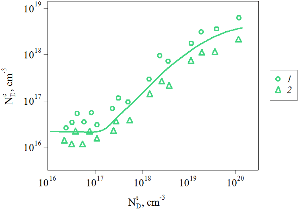
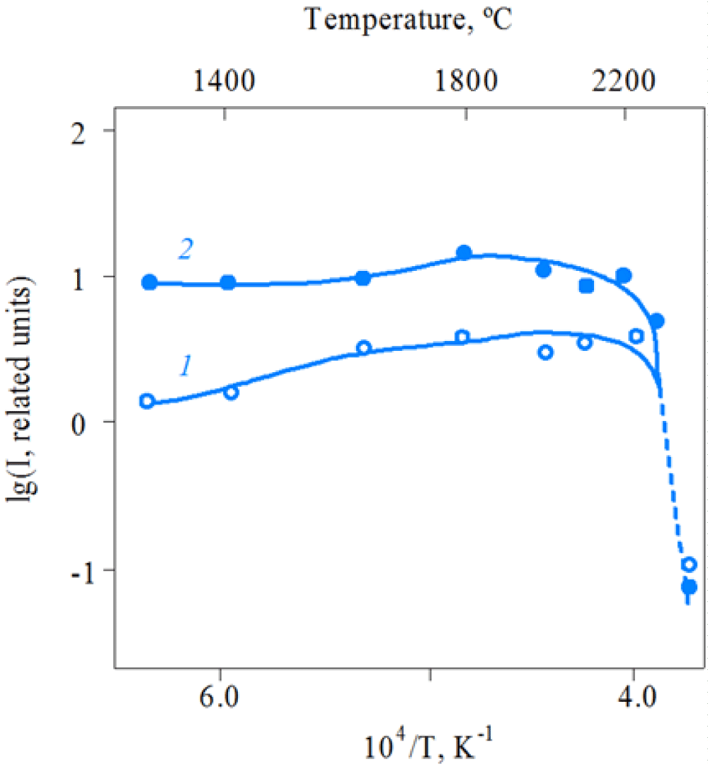
The dependence of the donor concentration in the LT SiC crystals grown in a Si-enriched system on the Nitrogen doping level in the SiC sources is presented in Figure 1. It is seen that at low impurity content, the donor concentration in SiC crystals ceases to depend on its concentration in the source. This result points to the possible presence of donor-type intrinsic defects in the SiC crystals.
This conclusion is confirmed by the fact that the concentration of paramagnetic nitrogen (main donor impurity) determined by the EPR in the high pure SiC samples is significantly lower than the donor concentration obtained from electrical measurements [9]. In the EPR spectra of the samples, additional lines are detected or nitrogen bands are split, which is associated with intrinsic defects [10]. A decrease in the nitrogen concentration (NcD) in LT SiC below 1×10¹⁷ сm-3 does not lead to the increase in diffusion lengths of the minority current carriers.
In the purest SiC samples, a characteristic luminescence with the D1 spectrum occurs, which is observed usually in the crystals irradiated with high-energy particles, and is caused by an intrinsic defect [9]. The study of optical absorption in LT SiC reveals a number of features not related to impurities. These features are similar to those found in irradiated samples [10] but are not observed in n-type HT 6H-SiC samples grown at temperatures as high, as 2500–2600 °C.
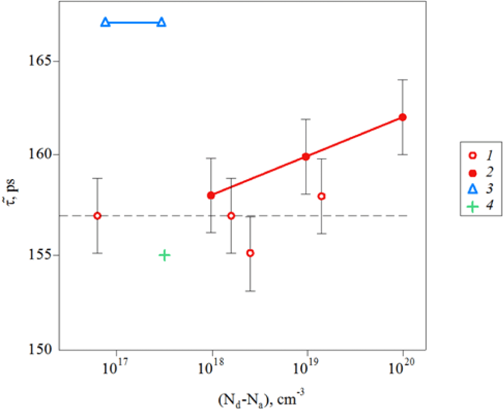
Positron annihilation spectroscopy (PAS): Girka, et al. [11] studied vacancy defects in as-grown LT- and HT-SiC crystals by PAS. The positron lifetime measurements in various SiC samples are shown in Figure 2.
The longest positron lifetimes, τB = 167 ps, are observed in Si-rich LT samples (Figure 2). Since the PAS method is sensitive mainly to vacancy defects, we can assume that positrons are trapped at the vacancy defects or their complexes with impurity atoms. The average positron lifetime (τ) in n-type HT 6H-SiC samples (Figure 2) is identical within the experimental error limits, irrespective of the donor impurity concentration. The corresponding spectra are well described by a single decay exponential with a time constant τB = (157±3) ns, where τB is the positron lifetime in the defect-free matrix.
In heavily p-type Al-doped samples, the positron lifetimes are higher than in the n-type, and τ increases with increasing concentration of the acceptor impurity. The lowest values of τ are obtained in the С-rich SiC (Figure 2). It means that C-rich and HT 6H-SiC samples contain the minimum concentration of the vacancy-type centers.
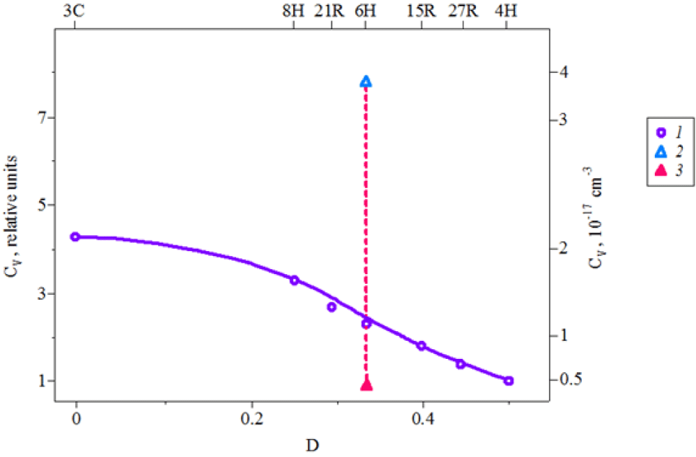
The ionization energy of native defects in SiC is generally high (Ei > 100 meV) [12]. At the typical measurement temperature (T = 300 K), therefore, the fraction of neutral vacancies in an n-type sample is not expected to be less than 30–50%. Addition-ally, the data show that increasing the concentration of electrically active impurities (nitrogen or aluminum) to the maximum solubility levels (1020–1021 cm-3) also does not induce a significant increase in the positron lifetime. Thus, the positrons in crystals of the HT SiC are annihilated primarily in a defect-free matrix with a characteristic time constant τB = 157 ps. To estimate the density of vacancies, we use the Brandt trapping model [13]. From this model, we obtain the vacancy density (CV) in the LT Si-rich crystals about (3 – 5)×1017 cm-3.
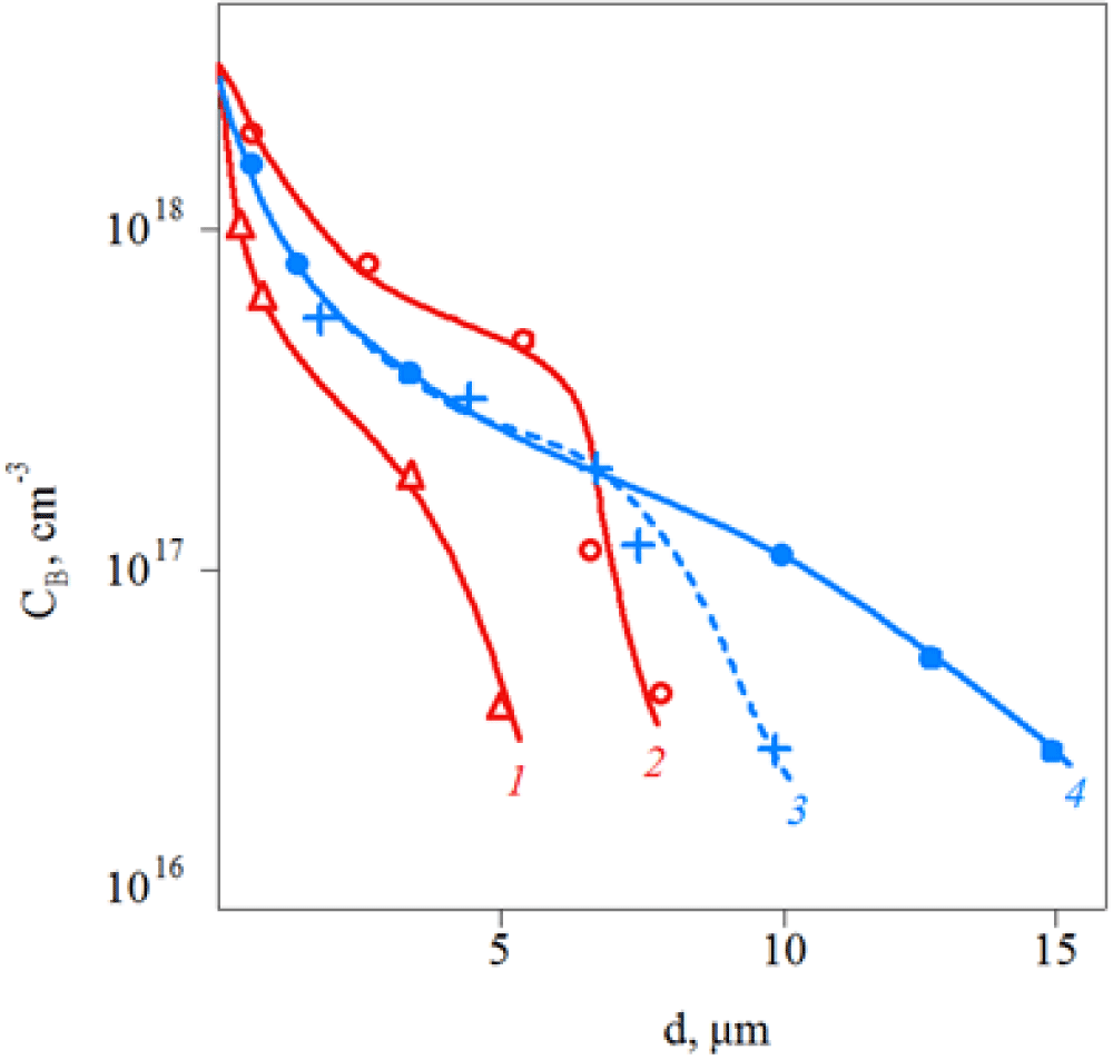
High-temperature diffusion: Additional information about the high-temperature state of defects is obtained using a comparative study of boron diffusion in the SiC samples grown under different conditions. The distribution of boron impurities in SiC samples grown under various conditions is shown in Figure 3.
It is seen that the maximum diffusion mobility of boron atoms was observed in the LT-samples grown in excess Si vapor. On the contrary, the minimum diffusion depth was noted in the HT and C-rich 6H-SiC samples. The pre-annealing of LT SiC samples at temperatures as high as 2450 °C led to a decrease in the diffusion depth in these samples (curve 3). An analysis of the data in Figure 3 shows that the diffusion coefficient of boron in LT SiC and HT samples differs by more than an order of magnitude. The bulk branch of the diffusion profile at low diffusion temperatures (Tdif) is described by the standard erfc function, and at high Tdif it becomes stepwise. The fast-diffusing state is known to be the (B-VC) pair [14]. Therefore, these experimental data confirm the increased concentration of VC in LT SiC. Defects introduced by diffusion are metastable and are partially annealed at high temperatures
A similar procedure is used for a comparative estimation of the vacancy density in the different SiC polytypes [15]. These results are also presented in Figure 4. It is seen, that the scatter of the vacancy density in different polytypes is much smaller than for crystals with different deviations from stoichiometry.
Based on the mentioned above it can be concluded that LT SiC samples contain an elevated density of intrinsic defects. It seems logical, to assume that the defects are vacancy clusters or complexes of vacancies with impurity atoms. From our point of view, the latter possibility is less probable, because positron-sensitive defects are observed in high pure SiC samples. Additionally, a change in the impurity doping level does not increase the intensity of the long-life component. At the same time, clusters of vacancies have a very high thermal stability in SiC.
Attempts to detect vacancy centers by PAS mean that crystals grown in a relative excess of carbon or in samples with high doping levels by donor impurities have been fruitless. However, the latter method allowed us to establish that silicon vacancies (VSi) carry a negative charge [16] and are typified by a comparatively long positron lifetime (τB = 260 ps). Consequently, these vacancies should be very efficiently detected by the PAS. However, VSi-related defects are not detected in the as-grown SiC, which obviously indicates a very low VSi density in such crystals.
Complexes of native defects in as-grown SiC crystals
D1-center: Intrinsic defects in as-grown crystals are also detected when studying the luminescent properties of LT SiC samples. The most interesting feature is the characteristic luminescence with the D1 spectrum (D1 PL), which was previously detected in the crystals irradiated with high-energy particles. Firstly, Vodakov, et al [17] showed that (D1 PL) can be observed not only in the irradiated samples but also directly in the as-grown crystals. D1 luminescence was detected in pure LT Si-rich samples grown at a high growth rate (Vg > 1.2 mm/h) [17, Figure 1].
An increase in the concentration of donor or acceptor impurities leads to a significant decrease in the intensity of the D1 PL. This indicates that the D1 spectrum is caused by recombination at the center, which includes only its intrinsic states and does not include Al, B, and N impurities. On the contrary, in the HT 6H-SiC samples, only impurity luminescence was observed with a maximum in the blue or orange spectral range, corresponding to the presence of Al or B impurities respectively. Thus, LT SiC possesses intrinsic defects responsible for the D1 PL spectrum. With high reliability it is possible to associate the formation of these luminescence-active defects with the relatively high concentration of carbon vacancies, the feature of the LT-SiC crystals.
In order to verify this conclusion, a series of experiments in which intrinsic defects were introduced into pure SiC crystals by diffusion from a highly doped p-type SiC(Al) epitaxial layer [17,18] were conducted. It is assumed that the p-type SiC contains a higher concentration of carbon vacancies VC, compared with the n-type SiC [5,6].
Verenchikova, et al. [18] studied the p-n–structures obtained by epitaxial growth of p+-SiC (Al) layers on the high-purity HT 6H-SiC substrates. The shift of the electroluminescence maximum to longer wavelengths in the structures grown at relatively low temperatures (Tg < 2200 °C) was observed. The assumed ionization energy of a deep donor center was about 0.6–1.0 eV [18].
Besides, the reverse breakdown voltage of such p-n junctions was much lower compared to theoretical values. The authors assumed that these features are connected with the formation of clusters of intrinsic defects. According to their calculation, the defect cluster includes about 60-70 atoms. The clusters were destroyed partly during high-temperature annealing at Ta > 2500 °C.
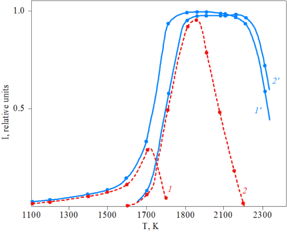
The thermal stability of the D1 centers was also studied by Vodakov, et al. [19]. Figure 5 represents the comparative dependences of the intensity of the D1 PL at the maximum of the spectrum on the annealing temperature of SiC samples containing D1 centers.
From Figure 5 it is readily seen, that the D1 PL is stable at temperatures as high, as 2200 °C. The luminescence decreases sharply only at Ta > 2300 °C, indicating a drop in the concentration of the D1 - centers.
It is of interest to compare the behavior of the D1-centers in the as-grown LT 6H-SiC and in the crystals irradiated with high-energy particles. For this purpose, LT 6H-SiC and HT 6H-SiC crystals with the same doping level, irradiated with reactor neutrons were studied [19]. The radiation dose was varied in the range F ~ 1017–1019 сm-2.
The intensity of the D1 PL of these samples via annealing temperature is shown in Figure 6, demonstrating that the D1 PL appears only after annealing. With increasing radiation doses (f) D1 PL occurs at higher Ta: (820, 1620 K respectively for F = 1017, 1019 cm-2) (Figure 6). It is seen, that luminescence intensity and annealing temperature of the D1 PL is higher in the LT than in the HT samples (Figure 6). It is noted that annealing temperature of D1 PL in highly neutron-irradiated LT SiC samples is about of 2000 °C that much lower than in the same as-grown crystals.
D-center (deep boron) – (EPR, DLTS, Phl measurements): Boron is widely used as an acceptor dopant in SiC and creates two levels in the band gap, corresponding to two different centers. The shallower center with an ionization energy Ei = 0.35–0.39 eV, is usually observed in electrical measurements in crystals doped with boron during HT-growth. This center is the isolated boron atom substituting a silicon in the SiC lattice. According to our EPR measurements [2], the second center with Ei = 0.7 eV is (BSi-VC) – pair, also known as D-center. This center attracts considerable interest, primarily because it is responsible for room-temperature luminescence (RT PL) with the peak in the yellow part of the spectrum in the case of the 6H-SiC (Em ~ 2.05 – 2.15 eV).
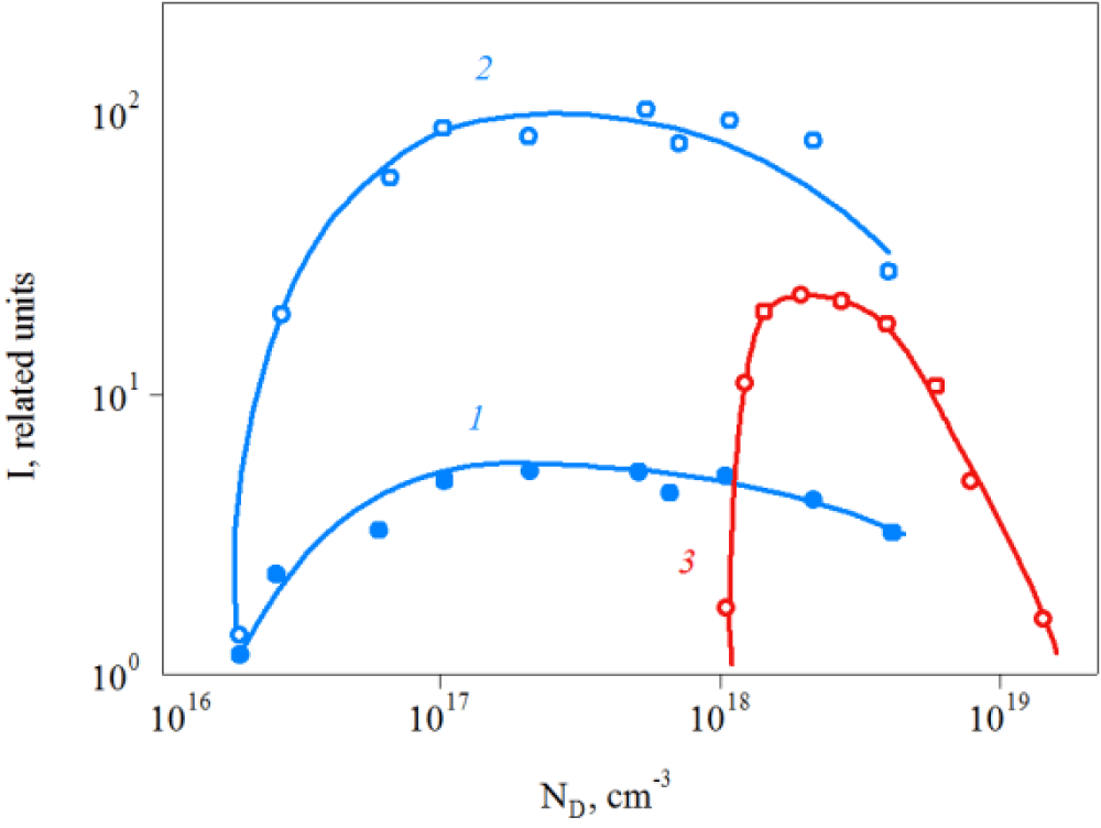
Vodakov, et al. [20] found that the intensity of this RT PL strongly depends on the growth temperature. The highest PL intensity was found in LT 6H-SiC samples (Figure 7), around one order of magnitude higher than in the HT SiC. It is possible to increase the intensity of the luminescence in HT 6H-SiC samples by boron diffusion, provided that the concentration of the donor nitrogen impurity ND > 1×1018 cm-3 (Figure 7).
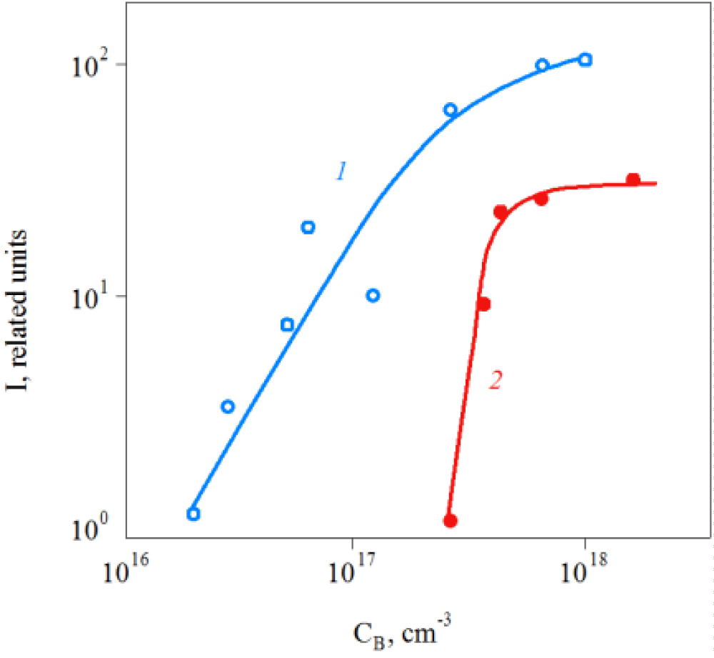
The intensity of the room temperature (RT) PL depends on the boron concentration. Nevertheless, regardless of the doping method, a higher RT PL intensity is achieved in LT SiC. The difference in RT PL intensity is especially significant when the boron impurity content is low (Figure 8).
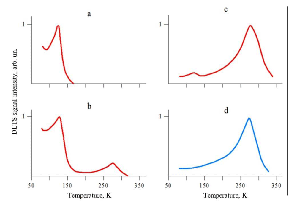
Both boron centers can be observed simultaneously by capacitance methods [21,22]. These centers were classified as В and D-centers, respectively. Ballandovich, et al. [21] studied DLTS spectra in the HT and LT SiC 6H samples doped with boron. DLTS curves measured on HT and LT 6H-SiC(B) samples are presented in Figure 9.
The DLTS measurements show that the B-centers are present in the all-initial SiC samples. The peak near 130 К on the DLTS spectra corresponds to these centers. The boron diffusion leads to a significant increase in the concentration of the В-centers. It also induces the appearance of the D-centers, with corresponding peaks on the DLTS spectra near 280 K (Figure 9 (b), (c), (d)), indicating the presence of the deep-level center). The relative concentrations of the D and В-centers are very sensitive to the growth method and to the conditions of the original samples doping.
In the HT 6H-SiC samples with an initial concentration of uncompensated donors below 6×1017 cm-3, doped by boron via diffusion we observe only В centers (Figure 9a). At a nitrogen concentration of 8×1017 cm-3, a weak signal of the D-center appears (Figure 9b), which becomes dominant at a nitrogen concentration of 2×1018 cm-3 (Figure 9c). In contrast with the HT 6H-SiC, the diffusion of boron into LT 6H-SiC with the same nitrogen concentration leads to the predominant formation of D-centers (Figure 9d). This behavior agrees well with the difference in the luminescence properties of the samples. Specifically, in the HT 6H-SiC samples (without D-centers), the RT PL is not observed. The crystals with (Nd–Na) > 1×1018 cm‑3 with the D-centers, exhibit a faint luminescence at room temperature. Finally, both the LT and HT samples with predominant concentrations of the D-centers, exhibit an intense room-temperature luminescence. These results confirm the conclusion that the D-centers are involved in the high-temperature boron luminescence.
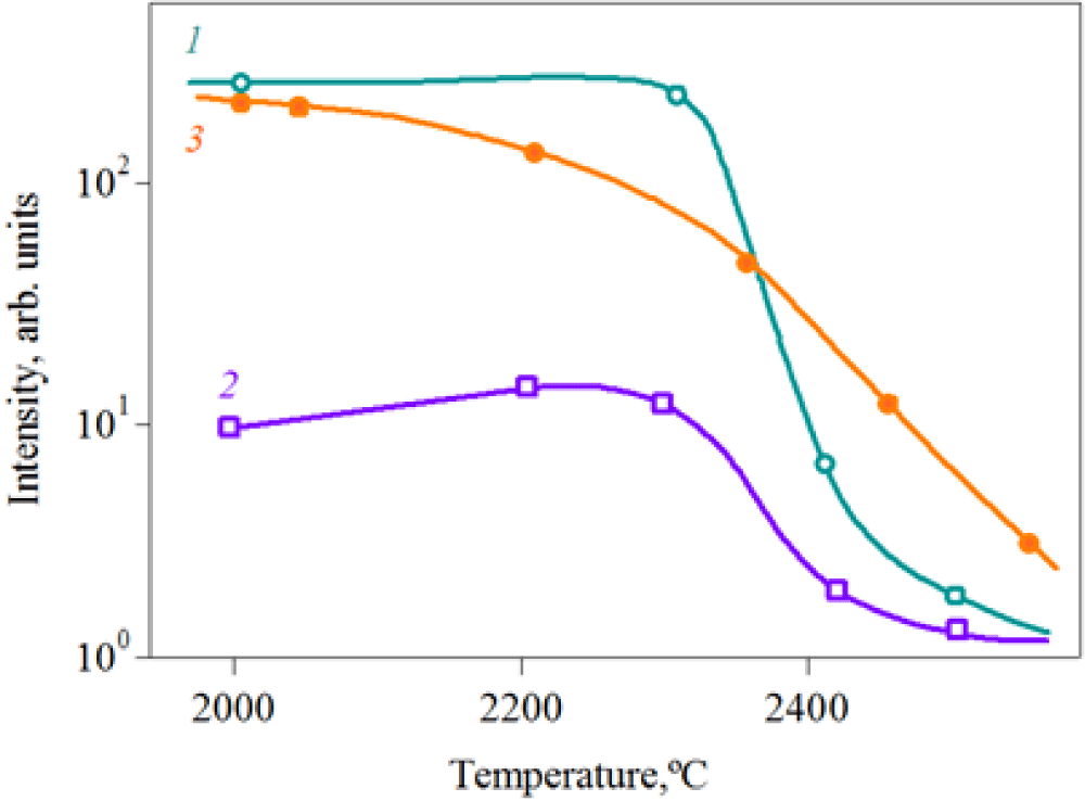
In [22], it was that the thermal stability of deep boron centers in LT and HT samples differs significantly. The dependence of the RT PL intensity on the annealing temperature for the HT (curve 1) and LT SiC (curve 3) samples doped with boron diffusion is shown in Figure 10. For comparison, the same dependence is shown for the initial LT-sample before boron diffusion (curve 2).
In all cases, high-temperature annealing leads to a decrease in the luminescence intensity. However, in LT 6H-SiC samples, the RT PL efficiency decreases more smoothly. As a result, the luminescence is kept up to higher annealing temperatures. The luminescent properties of the annealed LT 6H-SiC samples are regained upon the boron re-diffusion. However, if the annealing temperature exceeds 2500 °C, the boron diffusion into the samples with Nd<1018 cm-3 does not lead to the RT PL appearance, i.e. irreversible changes in the properties characteristic of LT samples occur, which become similar to HT samples.
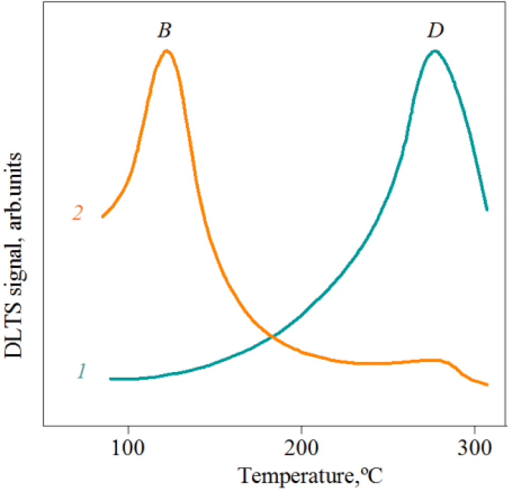
The analysis of DLTS spectra leads to the same conclusion (Figure 11). In Figure 11, curves 1 and 2 correspond to the DLTS spectra of the boron diffusion-doped LT sample measured before and after annealing at 2350 °C, respectively. These results indicate that the decrease in the RT PL efficiency upon high-temperature annealing is associated with the dissociation of D centers.
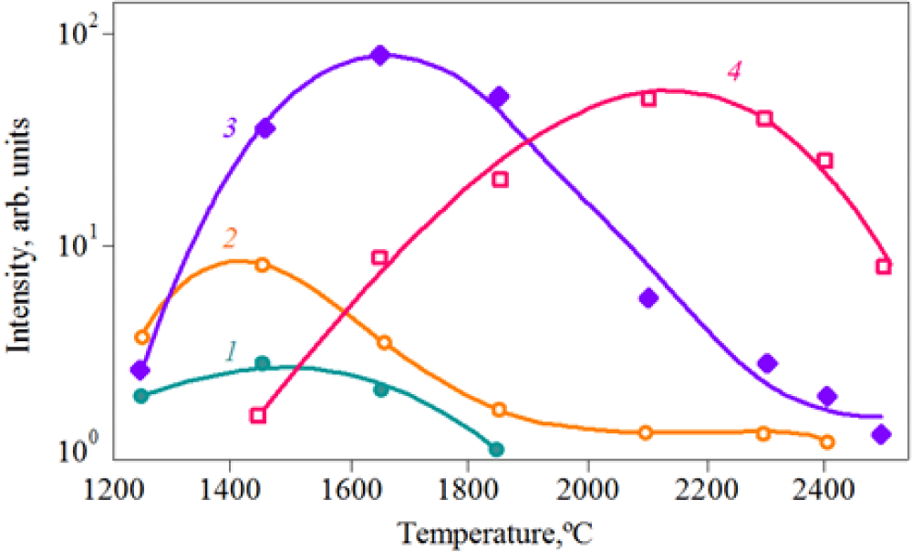
A decrease in the RT-PL intensity after high-temperature treatment is also observed in SiC samples irradiated with high-energy particles. Figure 12 demonstrates the annealing effect on the RT PL intensity for LT samples irradiated with electrons or reactor neutrons. An increase in the RT PL intensity in irradiated crystals with an increase in the annealing temperature is apparently due to the annealing of nonradiative recombination centers, and its subsequent decrease is due to the dissociation of the luminescence-active centers themselves.
At low doses of neutron irradiation of 1017–1018 cm–2, the RT PL intensity in HT samples begins to decrease already at temperature Ta ~ 1500–1600 ° C (Figure 12, curve 2). At nearly the same temperature, the RT PL is quenched in SiC crystals irradiated with high-energy electrons (see Figure 12, curve 1). With an increase in the irradiation dose, the RT PL quenching temperature rises sharply. At a dose of neutron irradiation Fn ≈ 1019 cm– 2, the RT PL centers are stable up to 1800 ° C, whereas at Fn ≈ 1020 cm–2, the RT PL appears only at ≈ 2100 ° C. At high irradiation doses of the order of 1021 cm–2, the RT PL is partially kept in the samples annealed at the maximum possible temperature for solid SiC, Ta ≈ 2600 ° C. From Figure 12, it is seen that with the irradiation dose increase, an increase in the intensity of RT PL is observed simultaneously with an increase in the annealing temperature. The data obtained indicate that D-centers, or boron–vacancy complexes (BSi–VC) are thermally unstable at temperatures above 1500 °C.
It is known that at the growth temperature of the LT 6H samples, the equilibrium vapor is highly enriched in silicon. The silicon content is almost an order of magnitude higher than the carbon content, which promotes the formation of D-centers. With an increase in the growth temperature, the partial pressures of silicon and carbon in the vapor phase become equal, which leads to a decrease in the content of carbon vacancies [10]. As a result, only B centers (isolated boron atoms in the silicon sublattice) are formed in HT 6H-SiC samples. Upon diffusion doping of SiC with boron, carbon vacancies formed on the surface are injected into the crystal in the form of B–VC complexes [14].
A similar effect of the Si: C ratio on the concentration of deep and shallow boron-containing acceptor centers was observed in 4H-SiC epitaxial layers grown by the CVD method [23]. As shown in the study [23], the concentration of shallow acceptor centers associated with boron in layers grown at a low Si:C ratio was two orders of magnitude higher than the concentration of D centers. In these layers, only low-temperature luminescence associated with shallow boron centers was observed. At the same time, the layers grown at a high Si:C ratio had an intense RT PL.
The high thermal stability of D-centers is evidently explained by the presence of clusters in the crystal, which are formed during growth or irradiation. Clusters also lead to a decrease in the apparent activation energy of annealing (Figure 10). Thus, the entire set of obtained data is explained as follows: deep boron-containing centers are metastable at temperatures above 1500 °C, and their retention at higher annealing temperatures is associated with the presence of clusters of intrinsic defects introduced into SiC crystals during growth, diffusion, or irradiation.
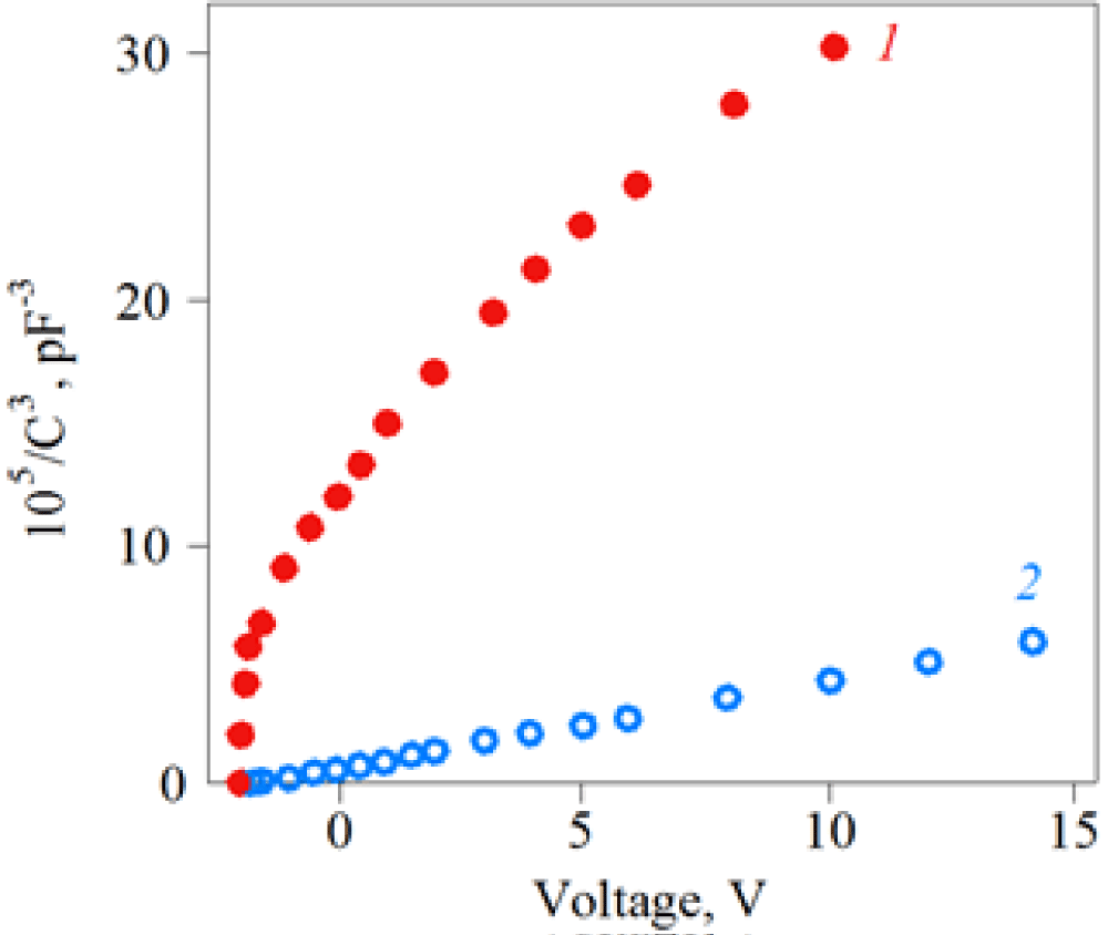
Thermal treatment of boron-doped samples affects not only their luminescent properties. High-temperature annealing of a diode structure with a boron-compensated base can change the concentration profile of the acceptor impurity near the p–n junction. Figure 13 shows capacitance-voltage (C–V) characteristics of p–n structures fabricated from a single sample - an aluminum-doped p+ epitaxial layer grown on an HT substrate with donor concentration Nd = 1.8×1018 cm–3. One of the boron-doped parts was subjected to a 5-min annealing at 2350 °C. Then mesa structures were formed on the basis of all the parts, with the Al contact (300 μm in diameter) to the p+ layer and the large-area Ni contact to the n-substrate. The C–V characteristics of structures subjected to boron diffusion and diffusion-annealing are shown in Figure 13 by curves 1 and 2, respectively.
As seen, when plotted in the (1/C2 – V) coordinates, the C–V characteristic of the control structure is linear, which is typical of p+–n junctions with a uniformly doped base. The slope of this characteristic is determined by the concentration of donors in the n-substrate, Nd = 1.8×1018 cm–3. Diffusion of boron into the starting sample leads to a many-fold decrease in the capacitance of the p+–n structure, with the capacitance depending only slightly on the reverse bias applied to the sample (Figure 13, curve 2).
It is known from the general theory that, in the case of a measuring bridge with a parallel equivalent circuit, a decrease in the equivalent capacitance of a sample may be due to an increase in the series resistance in the measuring circuit. However, we observed no frequency dispersion of capacitance, inherent in a diode with a high-resistivity base. The above specific features are characteristic of the behavior of a p–i–n structure, which in turn points to the presence in the vicinity of the p+–n junction of an extended, strongly compensated region.
DLTS measurements show that the appearance of this region is due to the introduction of D-centers by diffusion into the n-type substrate of the starting sample. Subsequent high-temperature annealing of the sample leads to the dissociation of the D-centers, with the capacitance of the structure again increasing (Figure 13, curve 2). This means that the annealing of D-centers causes an increase in the concentration of uncompensated donors in the diode base. This result is in agreement with the conclusion that part of the boron-related acceptor centers passes into an electrically inactive state in the course of annealing. The C–V characteristic of an annealed sample corresponds to the C–V characteristic of a p–n junction with a linear distribution of the impurity in the base, which is typical of diffusion structures.
Clusters of native defects: Experimental data obtained by various methods confirm the presence of intrinsic point defects in LT SiC crystals, primarily of the vacancy type. However, the reasons for the increased stability of these defects during thermal annealing remain unclear. It is assumed that this is due to the presence of active clusters. For LT 6H-SiC specimens grown in conditions of relative excess of silicon, faceted inclusions of unknown composition were observed by TEM [24]. This type of defect is absent in HT 6H-SiC crystals. High magnification permits visualization of scaly inclusions of the 2nd phase located in the center of such areas.
The results of the study show that LT 6H-SiC samples contain an increased concentration of intrinsic defects, which significantly affect the properties of the material. These defects are characterized by increased thermal stability and can be maintained at high temperatures during heat treatment. Additional information on clustering processes in SiC was obtained by studying the annealing of radiation defects [24-31].
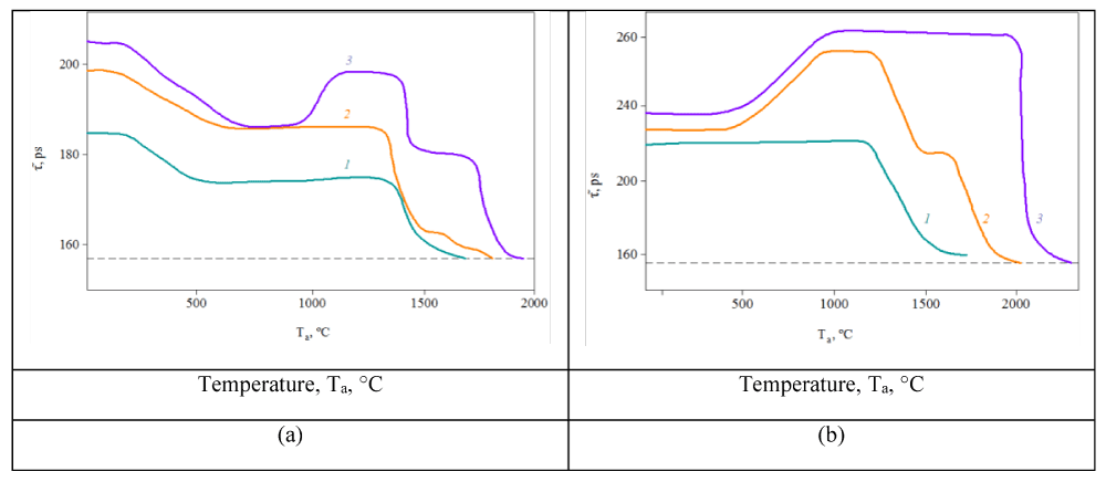
Girka, et al. researched the annealing of radiation defects in the SiC crystals, irradiated by fast electrons [25,26], reactor neutrons [27], and heavy ions [28] by positron annihilation spectroscopy (PAS). Figure 13 represents the dependence of the positron lifetime т of electron and neutron-irradiated samples on annealing temperature.
In general, one can distinguish up to five stages of positron-sensitive defect annealing: two low-temperature stages that are characterized by temperature interval ΔTa = 100 – 600 °C and defect migration activation energy Ea ≈ 1 eV; the stage of “negative” defect annealing (ΔTa = 1000–1200 °C, Еa = 1.9 eV); two high-temperature stages of defect annealing (ΔTa = 1400–1500°C and Ea = 2.2 eV, Тa = 1700–1900 °C and Ea = 2.8 eV, respectively).
The most interesting stage is the “negative” annealing stage. This stage is observed only in highly doped nitrogen samples. Comparison of the isochronous annealing curves of SiC crystals highly irradiated by neutron and electron fluencies suggests the same process in the “negative” annealing stage - the agglomeration of vacancies into vacancy clusters [25]. Cluster formation dependence on SiC nitrogen doping level allows us to consider that vacancy clusters are localized nearly the nitrogen atoms. Theoretical analysis of experimental data makes it possible to estimate the dimensions of the resultant clusters: they consisted of 5–8 vacancies and more than 20 vacancies. The maximum intensity of the long-lived component indicated that the cluster concentration reached a value of the order of 1018 cm-3. As can be seen from Figure 14, vacancy defects are annealed at temperatures above 1800–2000 °C. The annealing temperature increases with increasing the irradiation dose and nitrogen impurity content, which contributes to clustering.
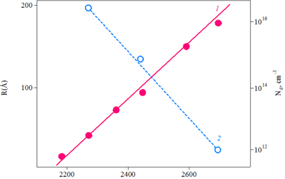
Kuitt, et al. [30] discovered another type of cluster in neutron-irradiated SiC by X-Ray diffractometry (XRD). Namely, it was shown that annealing at Ta = 1700 °C restored almost completely the electrical and optical properties of the SiC crystal. However, large clusters were detected by means of diffuse X-ray scattering. Any significant diffuse scattering associated with radiation defects was not observed immediately after irradiation. It appeared only after annealing at Ta > 1600–1900 °C. Approximate estimations based on the measured integral of the diffuse intensity gave an average defect size ranging from 100–200 Å at Ta = 1900 °C to 4000 Å at Ta = 2400 °C. The concentration of these defects decreased correspondingly from 3×10¹⁶ to 1×1012 cm-3 (Figure 15). Considering the high thermal stability of these clusters, it could be assumed that they include antisites or dislocated matrix atoms.
Sitnikova, et al. [31] studied neutron-irradiated SiC crystals by transmission electron microscopy. SiC samples irradiated with high doses (F=1020–1021 cm-2) of reactor neutrons and annealed at temperatures of 1800–2600 °C were used. The TEM method made it possible to observe separately the stages of annealing both vacancy and interstitial defects in the samples [31].
At low doses of irradiation of the SiC crystals (F ≈ 1020 cm-2) after subsequent annealing at Ta = 1800 °C, clusters with sizes no more than 40 nm are generated. Analysis of the image contrast of the defects suggests that these defects are small dislocation loops lying in prismatic planes. The concentration of these defects is 3×1014 cm-3.
The concentration of dislocation loops in the samples irradiated with high doses of neutrons F ≈ 1021 cm-2 increases by about an order of magnitude. The average size of the loops is 70–90 nm, but individual defects with sizes of about 150 nm are also observed. The analysis performed allows us to conclude about the vacancy character of the observed dislocation loops. This conclusion agrees with the results obtained by the PAS method [25], according to which the maximum size of vacancy clusters in irradiated SiC crystals is observed at an annealing temperature of Ta ≈ 1800 °C. Annealing temperature increase, above 2000–2300 ° C, results in defects disappearance is also observed by TEM.
Defects with black-and-white contrast in the samples irradiated with a dose of F ≈ 1021 cm-2 can also be observed after annealing at a temperature (Ta) of about 2300 °C. Analysis of these defects images shows that these are clusters of interstitial atoms. These defects are fairly evenly spread in the samples, and their concentration is (2–6)×1012 cm‑3. It should be noted that vacancy and interstitial dislocation loops lie in planes perpendicular to each other.
Summary information on detected intrinsic defects in SiC crystals is given in Table 2.
Thus, the experimental results indicate that metastable intrinsic defects are observed in SiC crystals grown by sublimation at moderate growth temperatures (below 2200 °C). Taking into account that under these conditions the equilibrium vapor composition is strongly Silicon enriched, one should expect the capture of excess components containing Sii, SiC, or VC. A theoretical analysis based on the energy calculation of the intrinsic defect formation shows that antisites and vacancies are the dominant defects in Si-rich samples [4,32]. Silicon antisite (SiC) is the main defect in the n-type Si, while the carbon vacancy (VC+) dominates in the p-type SiC [32]. At the growth temperature, the above defects are sufficiently mobile and form complexes or clusters. In this case, a significant part of the complexes are in electrically and optically active states, creating energy levels in the band gap.
Intrinsic electrical and optical active defects are detected primarily in high-purity LT 6H-SiC samples. The concentration of these defects does not exceed 1016 cm-3. The same intrinsic defects were found in Si-rich crystals grown by high-temperature chemical vapor deposition (HTCVD) [33], named P6/P7, Z1/2 and EH6/7 [6]. All these centers are very stable and anneal out at temperatures as high as 2000 °C.
We believe that the main intrinsic defects in LT SiC samples are carbon vacancies (VC), which are part of the D1 and D centers. Indeed, the conclusion that the D1-center includes VC is confirmed by EPR measurements [34]. PAS data show that vacancy defects in SiC are thermally stable and persist up to high annealing temperatures. The rapidly diffusing state of the boron impurity is the D-center or (BSisub>VC) complex. In this case, the heavily doped SiC of p-type conductivity may host the (BSVC) and (CSiVC) pairs, created by means of a high-temperature annealing. Our data indicate that native defects are not observed in carbon-rich SiC crystals. Obviously, this is due to the fact that neutral carbon antisites (CSi) are electrically non-active centers in SiC [12].
We show that deep boron (BSiVC) centers have high thermal stability and are preserved upon annealing to very high temperatures of 2500÷2600 °C. It is important to note that the annealing temperatures of the D-centers in as-grown crystals are significantly higher than those for the same centers created by irradiation. Boron diffusion data show that in the LT-samples these centers almost do not dissociate during diffusion at temperatures below 2400 °C. This is confirmed by the fact that at Td < 2200 0 C the boron impurity concentration profile in LT 6H-SiC is described by the standard erfc-function (Figure 3, curve 4). Contrary, in the HT 6H-SiC samples the steep part of boron distribution on the “tails” of diffusion profiles is observed, which indicates a sharp decrease in the relative concentration of D - centers (Figure 3, curve 2).
We associate the main difference between LT and HT 6H-SiC samples with the presence of clusters in LT SiC (or Si-rich crystals). During annealing, these clusters are in an active state, changing in size, up to extremely high temperatures of 2500÷2600 °C. Active clusters are the sources of non-equilibrium point defects [10]. Such a mechanism for the formation of intrinsic point defects was described in theoretical works and confirmed by experimental studies of the defects’ behavior in crystals containing radiation defects [34]. For example, it is known that Si vacancies are stable up to 750 0C, and C vacancies - up to 1150 °C. Nevertheless, they are actually found in SiC crystals at temperatures as high as 1400-1600 °C [34].
The highest cluster activity is observed at a relatively low growth temperature (below 2000 °C), when small clusters are predominate. The behavior of a system with non-equilibrium intrinsic defects is described within the framework of a well-known effect - Oswald ripening [35]. However, in contrast to classical semiconductor materials (for example, silicon) and metals, clusters in SiC remain in an active form at very high temperatures at which crystal growth occurs. Non-equilibrium defects are stable up to temperatures of the order of 2500 – 2600 °C, which is related to a low rate of relaxation processes in the bulk of the crystal. Thus, the relatively high concentration of electrically and optically active defects in SiC is a consequence of the presence of metastable active clusters. On the contrary, in HT and C-rich crystals, the clusters are obviously not sources of electrically active centers. According to theoretical calculations, the formation energies of carbon (ЕvС) and silicon (ЕvSi) vacancies in cubic position are 4.56 eV and 7.16 eV, respectively [32]. However, these values differ significantly from those obtained from the analysis of high-temperature diffusion processes in SiC. It is known that the activation energy of self-diffusion of C and Si atoms in n-type SiC lies in the range between 8.18 -8.2 eV [36,37] Since the migration energy of vacancies does not exceed 1.9–2.1 eV [10 ], we find that Ev is 6.2 eV, which is close to the calculated value of ЕvSi but noticeably exceeds ЕvС.
The values of the vacancy formation energies obtained from the analysis of the impurities diffusion are even less consistent. According to experimental data, the energies activation of diffusion for donor impurities of nitrogen and phosphorus are (7.6–9.3) eV [38] and 11.6 eV [39], respectively. These values are significantly higher than the diffusion activation energies for acceptor impurities (B, Al, Ga) which are about 5.1–6.0 eV [8].
Since donor impurities (N and P) migrate over carbon vacancies whereas the acceptor impurities over silicon vacancies [8] we can conclude that the formation energy of the carbon vacancies significantly exceeds the formation energy of the silicon vacancies. Indeed, according to calculations, the formation energies of carbon and silicon vacancies are 7–9 eV and 4–5 eV, respectively. These results significantly contradict the calculated data [32].
The low formation energy of silicon vacancies can be explained by the fact that the diffusion-active states of acceptor impurities are (VA) pairs that are stable at high temperatures. In the case of boron diffusion, this conclusion is confirmed. This assumption is supported by the fact that deep centers, which are complexes of impurity atoms with vacancies, are observed not only in SiC (B) but also in SiC samples doped with Al and Ga. Such samples of p-type conductivity contain significant concentrations of carbon vacancies, which obviously contributes to a decrease in the observed diffusion activation energy. Upon diffusion annealing, such layers are sources of vacancies responsible for the appearance of defect luminescence bands (D1 and D spectra).
At the same time, we believe that the higher values of the formation energy of carbon vacancies obtained from the analysis of high-temperature diffusion data are more reliable [40]. The high formation energies of equilibrium (thermal) point defects explain the fact that in a wide temperature range, the main mechanism of vacancy generation in LT 6H-SiC is cluster dissociation.
EPR of deep-level defects based on vacancies associated with impurity atoms
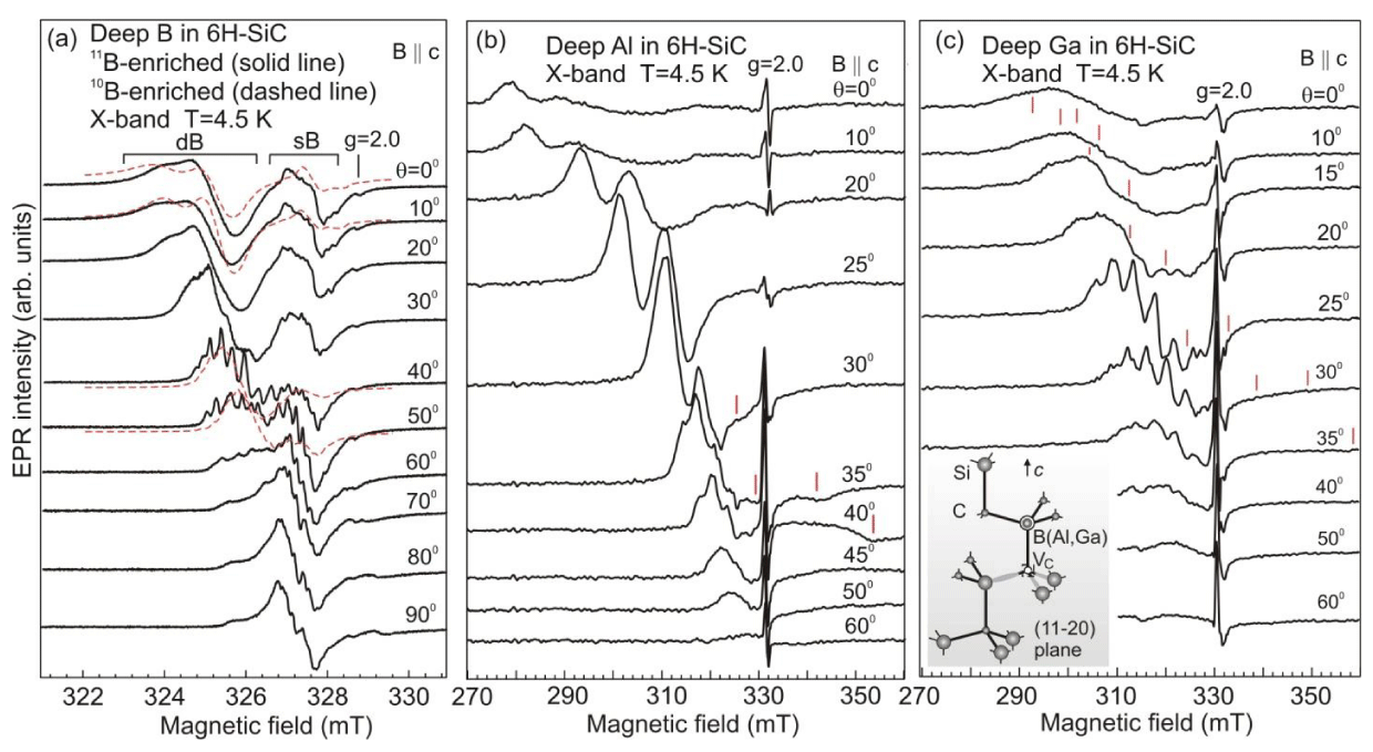
In this section, we will consider group-III acceptors with deep levels in SiC. Group-III elements (B, Al, and Ga) are the most important acceptor impurities in SiC. They may be introduced into a crystal either during the growth process, by diffusion, or by implantation. Results of EPR and ENDOR studies of group-III acceptors in SiC are summarized in the book [2]. Figure 16 shows the EPR spectra of deep B (a), deep Al (b), and deep Ga (c) in 6H-SiC crystal recorded in the X band (9.3 GHz) in various crystal orientations at 4.5 K. In Figure 16(a), the high-field signal denoted as sB and marked with a horizontal bar belongs to the shallow boron, since it can be described by a spin Hamiltonian with g factors and hyperfine (HF) structure parameters of shallow boron in two quasi-cubic and hexagonal positions in the lattice. In the low-field region at angles close to θ = 00 two unresolved overlapping broad lines are observed; they are denoted dB (deep B) in Figure 16(a). Their intensity correlates with the characteristic light-yellow luminescence and ODMR signals of deep boron centers.
Finding and determination of structure of Al acceptors with deep levels (deep Al) in SiC is of great interest concerning its application since aluminum is the main acceptor dopant in devices based on SiC. Appearing of Al acceptors with deep levels worsens the electric properties of a material; so the minimization of the content of deep aluminum in device elements is an important problem. Figure 16(b) shows the angular dependence of the EPR spectra in the 6H-SiC crystals doped with Al. The spectra consist of several groups of peaks which depend strongly on the angle between the field and the crystal axis c. One of the groups of anisotropic lines belongs to the shallow Al acceptors in inequivalent crystallographic positions. This group is seen in the low-field region in Figure 16(b) as two broad lines (in orientations close to B ||c). Vertical lines show the angular dependence of the ESR transitions of the shallow Al acceptors corresponding to cosθ. This behavior points to the fact that the shallow acceptors may be described within the effective mass approximation. Upon heating, the ESR signals of the shallow Al acceptors disappear above 5 K. The other group of anisotropic lines has angular and temperature dependences resembling those of the deep B. Thus, we will denote the new Al center as deep Al, analogous to the deep B. The signals of the shallow and deep Al acceptors can be distinguished by their angular dependences: the deep Al signals have a large intensity of up to 7 K while the shallow Al signals disappear at temperatures above 5 K. The difference in the peak positions for the shallow and deep Al is clear at angles exceeding 30. At orientations close to θ= 00 the signals of the shallow and deep Al overlap.
EPR spectra of deep gallium were observed in epitaxial layers of 6H-SiC doped with Ga. The spectra, which depend strongly on the angle between the crystal axis c and the magnetic field, are shown for different orientations of the field in Figure 16(c). Note a remarkable qualitative similarity between the EPR spectra of deep B (Figure 16(a)) and deep Al (Figure 16(b)) centers and the spectra observed in 6H-SiC doped with Ga (Figure 16(c)). Only differences in the parameters of the spin Hamiltonians were found. The spectra of the deep Ga centers are anisotropic, and the resolution of the HF structure increases as the crystal orientation deviates from the axis c. It was calculated to demonstrate that the resolved HF structure at angles exceeding 200 appears due to the HF interaction with nuclei of 69Ga and 71Ga. This analysis of the HF interaction with Ga showed definitely that the revealed defect contains one Ga atom. The ratio of the HF constants for deep Ga and B corresponds to that of theoretical constants of the HF interaction for Ga and B atoms.
Irrespective of the size of the group-III impurity atom comprising the deep center, either larger (Al, Ga) or smaller (B) than silicon, the physical behavior of the center and its microscopic model are the same. We suppose that the deep boron, deep aluminum, and deep gallium in the acceptor state are a pair of the group-III element and the carbon vacancy: ASi–VC, where A = B, Al, Ga. ASi stands for B (Al, Ga) substituting silicon, and VC is the carbon vacancy (Figure 16с). Arguments supporting this model are the following: the centers have almost axial symmetry relative to the axis c and a strong anisotropy; the HF interaction with the nuclei of B, Al, Ga has the same order of magnitude as for the shallow B (Al, Ga) acceptors which are impurity atoms replacing the Si atoms. Apparently, the position of the carbon vacancy along the axis c concerning the B, Al, and Ga impurity replacing silicon is energetically favorable.
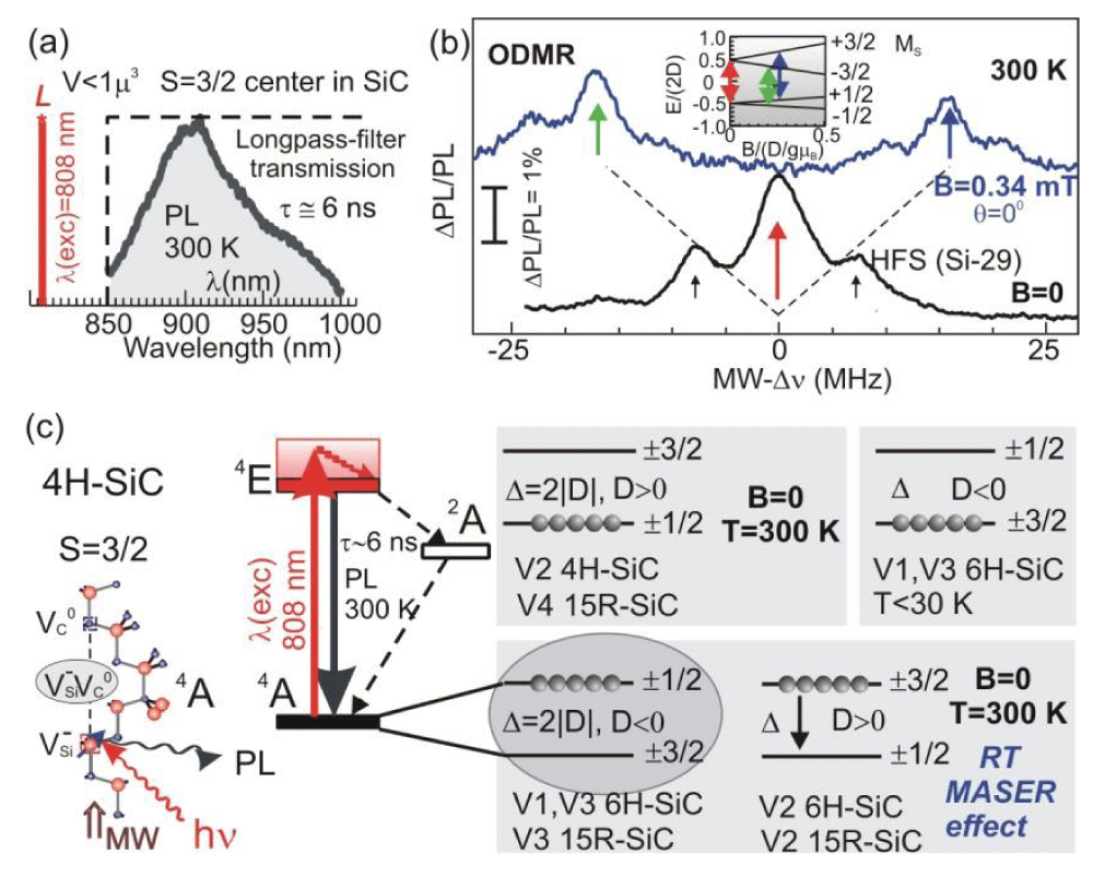
Spin defects in SiC as a material platform for sensing, quantum photonics, and information processing at ambient conditions: The unique quantum properties of NV centers in diamond [42] have motivated efforts to find defects with similar properties in silicon carbide, which can extend the functionality of such systems [2,43-46]. SiC is a technological material that is used in various devices. This material is now taking on a new role as a platform for using new quantum technologies. A feature of SiC is the presence of different polytypes, and the properties of atomic-scale defects are unique for each polytype; moreover, even in one polytype, the center can occupy different nonequivalent lattice positions. This allows one to select a center with optical and microwave parameters suitable for a specific task. Atomic-scale defects in SiC are considered a material platform for applications in photonics, spintronics, quantum information processing, and environmental sensing. The spin state of the defects can be initialized, manipulated, and read out by means of ODMR, via LAC and CR [47–57]. The presence of high concentrations of isotopes with zero magnetic moments in silicon carbide provides good coherent properties for spin defects. As a result, coherent manipulations with spin states were performed at room temperature and even at temperatures exceeding room temperature. Two families of defects were found in silicon carbide: the first with the spin S = 1 and the second with the spin S = 3/2. For both families, a unique property of optical alignment of the populations of spin sublevels was discovered, which made it possible to perform spin manipulations by changing the populations of these sublevels using resonant microwave irradiation. Such manipulations lead to giant changes in the photoluminescence of defects, which makes it possible to register magnetic resonance by optical methods. The center with spin 1 is a neutral divacancy of silicon and carbon located in adjacent positions with a covalent molecular bond. A model is proposed for a spin 3/2 defect in the form of a negatively charged silicon vacancy in the paramagnetic state, which is perturbed by the interaction with a neutral carbon vacancy in a nonparamagnetic state located at a neighboring site along the SiC symmetry axis [54]. These centers are usually designated by the corresponding zero-phonon lines (ZPLs). For this family, the ground state and the excited state have spin S = 3/2. For a number of defects, the population inversion in the ground state is created even in zero magnetic fields, and at room temperature using optical pumping, which leads to stimulated microwave radiation.
Figure 17 (a) shows an example of the room temperature photoluminescence (PL) spectra of spin-3/2 centers in SiC (see Chapter 6 in Ref. [2]). Figure 17 (b) presents a typical experimental microwave (MW) dependence of the ODMR signal of the spin-3/2 centers in SiC, Δν is the zero-field splitting (ZFS). The ODMR signal is detected under laser excitation λ = 808 nm in zero and B=0.34 mT magnetic fields. The vertical bar indicates the ODMR contrast. A hyperfine structure (HFS) due to the interaction with 29Si nuclei for twelve Si atoms in the next nearest-neighbor shell of the Si vacancy is shown by arrows. The inset shows the energy level diagram and corresponding resonance transitions. The schemes of optically induced alignment of spin level populations in a zero magnetic field at room temperature for spin-3/2 centers (possible configuration is depicted) in different SiC polytypes are shown in Figure 16 (c).
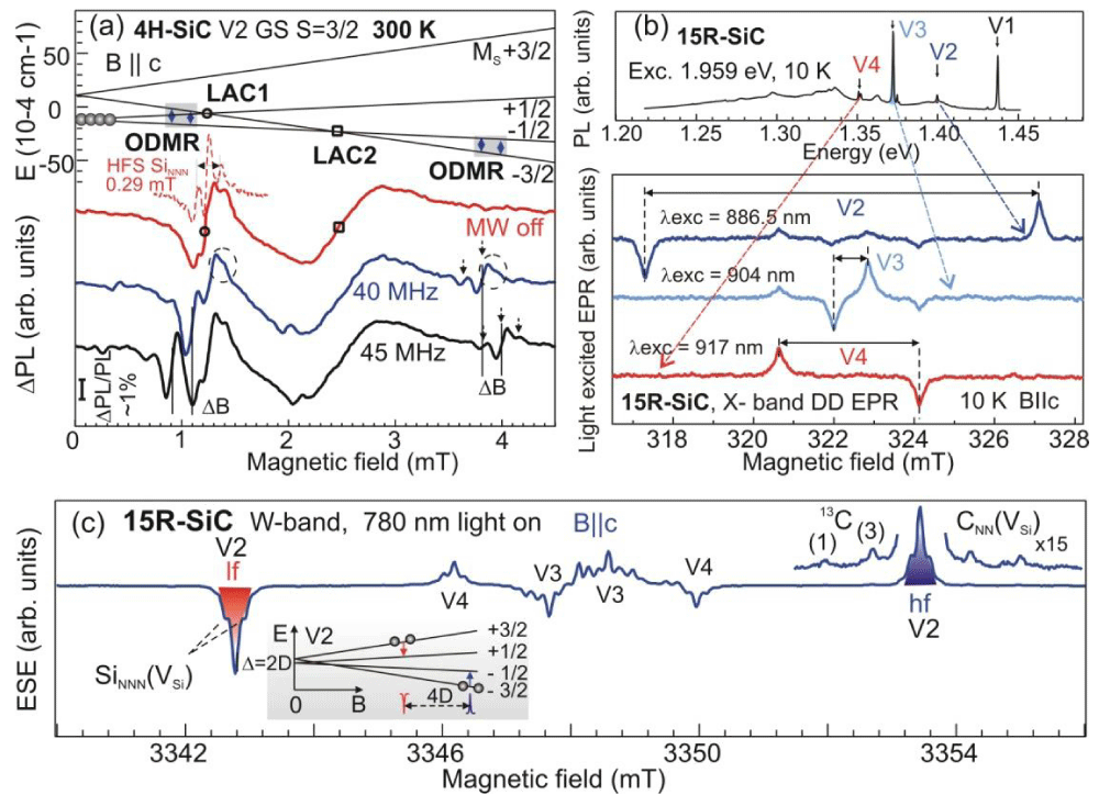
Figure 18 (a), as an example, shows signals of room temperature ODMR and level anti-crossing (LAC) of the V2 spin centers in a 4H-SiC crystal (see [2]). The signals were recorded by lock-in detection of the change in the PL in the near-IR range with the application of a constant magnetic field and an oscillating low-frequency magnetic field. The energy of the corresponding spin levels is shown at the top. The LAC in the absence of the MW field (MW “off”), denoted as LAC1 and LAC2; for LAC1 B=D and for LAC2 B=2D, where ZFS Δ=2|D|, and two ODMR signals recorded at the MW field on 40 and 45 MHz are shown.
The choice of frequencies was due to the fact that when the ODMR signal approaches the LAC1 signal, the ODMR signal increases several times and approaches the LAC1 signal intensity. The ODMR line shift ΔB at frequencies of 40 and 45 MHz is shown demonstrating the principle of measuring magnetic fields by the ODMR method. A magnetic-field position of the LAC1 signal of spin-3/2 centers in the ground state weakly depends on the orientation of the crystal, and therefore LAC1 signal is narrow enough in powder SiC. Thus, the LAC1 signal of spin-3/2 centers in nanosized samples of SiC can be used for all-optical measuring of magnetic fields with submicron spatial resolution. The temperature-dependent position of the LAC1 signal of spin-3/2 centers in an excited state can be used for all-optical measuring of temperature with submicron spatial resolution.
It is assumed that if the ODMR signal coincides with the LAC, polarization of the surrounding silicon 29Si and 13C carbon nuclei with long relaxation times is possible through hyperfine interactions. Circles indicate areas of reduction of the signals with a certain polarization of 29Si, which are present in the signals of the ODMR in the form of satellites. We assume that optical registration of nuclear magnetic resonance on polarized nuclei 29Si and 13C of spin centers in SiC will find a number of applications (quantum computing, NMR imaging, gyroscopes, etc). In Figure 18 (b), the PL zero-phonon lines (ZPLs) in 15R-SiC of the corresponding spin-3/2 centers (top) and X-band direct-detected (DD) EPR spectra induced with ZFLs V2, V3 and V4 (bottom) are demonstrated. In Figure 18 (c), optically induced ESE spectra measured in 15R-SiC at W-band (94 GHz) are shown; the light-induced inverse population of the spin sublevels of V2 centers is depicted in the inset [54].
A spin ensemble of defects can be prepared in a coherent superposition of states, while Rabi oscillations in SiC can be maintained at room temperature up to fractions of a millisecond. The electron spin of defects can be controlled using a low-energy microwave field with a frequency of 1–300 MHz, which is compatible with NMR imaging. Vacancy defects in SiC are optically active in the near-infrared, which is preferred for potential biological applications in vivo due to its deepest tissue penetration and which is compatible with fiber optics. The sensing concept is based on variants of the ODMR method with sensitivity up to a single spin [2,46,47]. The demonstrated spin properties of defects in SiC and related nanostructures open up new possibilities for modern quantum technologies and the creation of quantum sensors for submicron probing. The effect of optically induced population inversion of spin states at RT can be used to create solid-state masers and highly sensitive radio frequency amplifiers.
Recently, the existence of NV defects (NC-VSi) in SiC has been demonstrated in [58,59] and can be expected to hold similar promising properties as NV defects in diamond and divacancies in SiC. In the negative charge state, they have S=1, its optical properties shifted to the NIR region (around 1200-nm wavelength).
The behavior of point defects and their clusters forming with deep levels in SiC band gap together with shallow and deep acceptors properties, considered in the current manuscript is of significant importance for the development of quantum technologies with defect spins. The latter is well documented in the case of the negatively charged nitrogen-vacancy defect in diamond for which the doping levels with donor and acceptor impurities, the presence of other point defects in the lattice plays a crucial role on the NV defect charge stability, optical properties and spin-coherence times [60,61]. The same is true for VSi defects in SiC [62]. That is results presented in the current manuscript are of significant importance.
The EPR and photoluminescence spectra of erbium centers Er3+ associated with a carbon vacancy (Er3+–VC) were found in SiC [2]. Er3+ ions occupy a special place in optical communication since the energy of the transition inside the 4f-shell of this ion corresponds to a wavelength of 1.54 μm, which corresponds to the minimum absorption in fiber-optic communication systems. Qubits based on nuclear spins in solids, as a rule, have a high degree of coherence, which allows them to be used as systems for storing and processing quantum information. The electron-nuclear spin system for Er3+ in SiC is of particular interest, since both the electron spin and the nuclear spins of the 29Si and 13C isotopes have minimum values (1/2), while it is possible to change the isotopic composition of the nuclear spins of silicon and carbon, as well as changes in the isotopic composition of erbium. Due to the large electronic g-factor for the Er3+ ion [2], there is a strong interaction with resonant microwave excitation in EPR. The electronic and nuclear spins interact. The spin of an electron can be strongly excited through optical or microwave channels to create certain quantum states. The information can then be mapped into the nuclear spin of the ligand (29Si and 13C) to implement long-lived qubit memory.
Conclusion
Native defects in SiC crystals grown at low temperatures below 2200 °C in a Si-rich system were discovered. These defects affect on electrical and optical properties of the material and the quality of p-n-junctions. They are complexes that include a carbon vacancy. The same defects also appear in SiC crystals containing radiation defects. We note that the high thermal stability of intrinsic defects in as-grown crystals in comparison with similar radiation defects is explained by the presence of active clusters in crystals, which are sources of mobile point defects at elevated temperatures. Experimental evidence has been obtained of the presence of such clusters, which are retained upon annealing to temperatures as high as 2500–2600 °C. That is results presented in the current manuscript are of significant importance. Quantum technologies based on coherent control of the spins of color centers in silicon carbide have developed fantastically over the past decade. The combination of supersensitive optical techniques for high-resolution image detection and reliable coherent control using magnetic resonance are key components in the development of the first quantum devices based on these materials. The possibility of highly accurate scaling of color centers and achieving long coherence times opens up new prospects for so-called hybrid quantum processes, in which color centers are associated with different types of qubits. There is no doubt that this area of research will develop rapidly in the near future and, as can be expected, will lead to the emergence of new quantum technologies.
Author contributions
Conceptualization, Evgeniy Mokhov, Pavel Baranov. Data curation, Evgeniy Mokhov, Pavel Baranov, Olga Kazarova. Writing – original draft, Evgeniy Mokhov, Pavel Baranov, Olga Kazarova.
The authors acknowledge the support of state assignments of the Ministry of Science and Higher Education of the Russian Federation to the Ioffe Institute (0040-2019-0016).
- Handbook of silicon carbide materials and devices / edited by Zhe Chuan Feng, First edition., Boca Raton : CRC Press, (2023);
- Baranov PG, Bardeleben HJ, Jelezko F, Wrachtrup J. Magnetic Resonance of Semiconductors and Their Nanostructures. Springer Series in Materials Science. 2017; 253.
- Whiteley SJ, Wolfowicz G, Anderson CP , Bourassa A, Ma H, Ye M, Koolstra G , Satzinger KJ, Holt MV , Heremans FJ, Cleland AN , Schuster DI , Galli G, Awschalom DD. Spin–phonon interactions in silicon carbide addressed by Gaussian acoustics Nature Physics. 2019; 15: 490-495.
- Castelletto S, Peruzzo A, Bonato C, Johnson BC, Radulaski M, Ou H, Kaiser F, Wrachtrup J. Silicon Carbide Photonics Bridging Quantum Technology. ACS Photonics. 2022; 9: 1434-1457.
- La Via F, Camarda M, La Magna A. Mechanisms of growth and defect properties of epitaxial SiC. Appl Phys Review. 2014; 1: 031301.
- Lшvlie LS. Intrinsic bulk and interface defects in 4H silicon carbide. Series of dissertations submitted to the faculty of Mathematics and Natural Sciences, University of Oslo No. 1205 ISSN 1501-1710 (2012)
- Vodakov YuA, Mokhov EN. Growth of semiconductor SiC. Patents: USSR N 403275 (1970); France: No 2 264 589 (1975); UK:No 1458445 (1977), FR Germany: No 24 09 005 (1977); USA No 414572 (1979);
- Mokhov EN. Doping of SiC crystals during sublimation growth and diffusion. In Book: Crystal growth. Intech Open. 2018, edited by: Dr. Vadim Glebovsky
- Mokhov EN, Ramm MG, Vodakov YuA. Growth of Silicon Carbide epitaxial layers – Visokochistie Materiali (in Russian). 1992; 3: 98-105.
- Vodakov YuA, Mokhov EN. Point Defects in Silicon Carbide. Inst Phys Conf Ser.1994; 137(3): 197–206.
- Girka AI, Mokhov EN. Vacancy defects in Silicon Carbide. Phys Sol St. 1995; 37(11): 1855-1859.
- Bernardini F, Mattoni A, Colombo L. Energetics of native point defects in cubic silicon carbide. European Phys Journal. 2004; 38B: 437–444.
- Brandt W, Paulin R. Positron diffusion in solids. Phys Rev. 1972; B5: 2430–2435.
- Mokhov EN, Vodakov YuA, Lomakina GA, Oding VG, Kholuynov GF, Semenov VV. Diffusion of Boron in Silicon Carbide. Sov Phys Semicond. 1972; 6(3): 414–419.
- Vodakov YuA, Lomakina GA, Mokhov EN. Nonstoichiometry and polytypism Silicon Carbide. Sov Phys Sol St. 1982; 24(5):780–784.
- Wang C, Bernholc J, Davis RF. Formation energies, abundances, and the electronic structure of native defects in cubic SiC. Phys Rev B Condens Matter. 1988 Dec 15;38(17):12752-12755. doi: 10.1103/physrevb.38.12752. PMID: 9946240.
- Vodakov YuA, Lomakina GA, Mokhov EN, Oding VG, Ramm MG, Sokolov VI. Appearance of defect luminescence with a D1 spectrum in 6H-SiC upon generation of excess carbon vacancies. Sov Phys Semicond. 1986; 6(8): 900–903.
- Verenchikova RG, Vodakov YuA, Litvin DP, Mokhov EN, Ramm MG, Sankin VI, Ostroumov AG, Sokolov VI. Electrical properties of SiC р-п-Junctions with epitaxial р+-type layer doped with Аl. Sov Phys Semicond. 1982; 18(11): 1309–1311.
- Vodakov YuA, Lomakina GA, Mokhov EN, Ramm MG, Sokolov VI. Influence of growth conditions on the thermal stability of defect luminescence with spectrum D1 in neutron-irradiated 6H-SiC.Sov. Phys. Semicond. 1986; 6(8): 1347–1350.
- Vodakov YuA, Goncharov EE, Lomakina GA, Maltsev AA, Mokhov EN, Oding VG, Ramm MG, Rybova GG. Features of high-temperature luminescence of boron-doped SiC epitaxial layers. Sov Phys Semicond. 1987; 21(2): 126–130.
- Ballandovich VS, Mokhov EN. Capacitive spectroscopy of boron-doped SiC - Sov.Phys. Semicond. 1995; 29(2): 126-130.
- Ballandovich VS, Mokhov EN. Annealing of deep boron centers in SiC. Semicond. 2002; 36(2): 160–166.
- Sridhara SG, Clemen LL, Devaty RP, Choyke WJ, Larkin DJ, Kong HS, Troffer T, Pensl G. Photoluminescence and transport studies of boron in 4H SiC. J Appl Phys. 1998; 83(12): 7909–7919.
- Mokhov EN, Radovanova EI, Sitnikova AA. Investigation of Structural Defects in SiC Crystals by Transmission Electron Microscopy. Springer Proceed Phys.1992; 56: 231–236.
- Girka AI, Mokrushin AD, Mokhov EN, Osadchiev VM, Svirida SV, Shishkin AV. J Sov. Phys. JETP 70,322 (1990).
- Girka AI, Kuleshin VA, Mokrushin AD, Mokhov EN, Svirida SV, Shishkin AV. Positron diagnostics of vacancy defects in electron-irradiated SiC - Sov Phys Semicond. 1989; 23(7): 790–796.
- Girka AI, Kuleshin VA, Mokrushin AD, Mokhov EN, Svirida SV, Shishkin AV. Positron diagnostics of vacancy defects in neutron-irradiated SiC. Sov Phys. Semicond. 1989; 23(12): 1337–1340.
- Girka AI, Didin A, Yu, Mokrushin AD, Mokhov EN, Svirida SV, Shishkin AV, Shmarovoz VG. Clustering of vacancies during thermal annealing of SiC irradiated with heavy ions - Sov. Techn Phys Lett. 1989; 15(12): 24-27.
- Girka AI, Mokrushin AD, Mokhov EN, Svirida SV, Shishkin AV. Positron diagnostics of Radiation Defects in SiC. Springer Proceed. in Phys.1992; 56: 207-212.
- Kutt RN, Lcpneva AA, Lomakina GA, Mokhov EN, Tregubova AS, Scheglov ММ, Yuldashev GF. Defect forming at annealing of neutron irradiated SiC. Sov Phys Sol St. 1988; 30(9): 2606–2609.
- Sitnikova AA, Mokhov EN, Radovanova EI. TEM Investigation of Radiation Defects in SiC Crystals. Phys St Sol. 1993; 135a(2): k45–49.
- Kobayashi T, Harada K, Kumagai YU, Fumiyasu Oba, Yu-ichiro M. Native point defects and carbon clusters in 4H-SiC: A hybrid functional study. J. Appl. Phys. 2019; 125(12): 125701.
- Janzen E, Son NT, Magnusson B, Ellison A. Intrinsic defects in high-purity SiC. Microelectronic Engineering. 2006; 83 (1): 130-134.
- Eva Rauls. Annealing mechanisms of point defects in Silicon Carbide Theoretical Investigation. Dissertation zur Erlangung des akademischen Grades Paderborn. 2003; 119.
- Uematsu MM. Simulation of Transient Enhanced Diffusion of Boron Induced by Silicon Self-Implantation. Jpn. J. Appl. Phys. 1997A; 36(8): 982-L985.
- Hong JD, Davis RF. Self-diffusion of C-14 in high purity and N-doped a-SiC single crystals. J. Am. Ceram. Soc. 1980; 63(9,10): 546-52.
- Hong JD, Davis RF, Newbury DE. Self-diffusion of Si-30 in a-SiC single crystals. J. Mat. Sci. 1981; 16(9): 2485-2494.
- Kroko LJ, Milnes AG. Diffusion of nitrogen in SiC, doped Al. Sol. St. Electrn. 1966; 99(11/12): 1125-1134.
- Mokhov EN, Gornushkina ED, Didik VA, Kozlovskii VN. Diffusion of phosphorus in Silicon Сarbide. Sov. Phys.: Sol. St. 1992; 34(6): 1043-1045.
- Rüschenschmidt K , Bracht NH, Stolwijk A. Self-diffusion in isotopically enriched silicon carbide and its correlation with dopant diffusion. J. Appl. Phys. 2004; 96: 1458-1463. https://doi.org/10.1063/1. 1766101
- Il`in IV, Uspenskaya YA, Kramushchenko DD, Muzafarova MV, Soltamov VA, Mokhov EN, Baranov PG. Group III Acceptors with Shallow and Deep Levels in Silicon Carbide: ESR and ENDOR Studies, Phys. Solid State. 2018; 60( 4): 644-662.
- Gruber A, Dräbenstedt A, Tietz C, Fleury L, Wrachtrup J, von Borczyskowski C. Scanning Confocal Optical Microscopy and Magnetic Resonance on Single Defect Centers Science. 1997; 276: 2012-20142.
- Baranov PG, Il’in IV, Mokhov EN, Muzafarova MV, Orlinskii SB, Schmidt J. EPR identification of the triplet ground state and photoinduced population inversion in SiC.JETPLett. 2005; 82: 441.
- Baranov PG, Bundakova AP, Borovykh IV, Orlinskii SB, Zondervan R, Schmidt J. Spin polarization induced by optical and microwave resonance radiation in a Si vacancy in SiC: A promising subject for the spectroscopy of single defects. JETP Lett. 2007; 86(3): 202-206.
- Weber JR, Koehl WF, Varley JB, Janotti A, Buckley BB, Van de Walle CG, Awschalom DD. Quantum computing with defects. Proc Natl Acad Sci U S A. 2010 May 11;107(19):8513-8. doi: 10.1073/pnas.1003052107. Epub 2010 Apr 19. PMID: 20404195; PMCID: PMC2889300.
- Baranov PG, Bundakova AP, Soltamova AA, Orlinskii SB, Borovykh IV, Zondervan R, Verberk R, Schmidt J. Silicon vacancy in SiC as a promising quantum system for single-defect and single-photon spectroscopy. Phys. Rev. B 2011; 83: 125203.
- Riedel D, Fuchs F, Kraus H, Väth S, Sperlich A, Dyakonov V, Soltamova AA, Baranov PG, Ilyin VA, Astakhov GV. Resonant addressing and manipulation of silicon vacancy qubits in silicon carbide. Phys Rev Lett. 2012 Nov 30;109(22):226402. doi: 10.1103/PhysRevLett.109.226402. Epub 2012 Nov 27. PMID: 23368138.
- Kraus H, Soltamov VA, Fuchs F, Simin D, Sperlich A, Baranov PG, Astakhov GV, Dyakonov V. Magnetic field and temperature sensing with atomic-scale spin defects in silicon carbide. Sci Rep. 2014 Jul 4;4:5303. doi: 10.1038/srep05303. PMID: 24993103; PMCID: PMC4081891.
- Kraus H, Soltamov VA, Riedel D, Väth S, Fuchs F, Sperlich A, Baranov PG, Dyakonov V, Astakhov GV. Room-temperature quantum microwave emitters based on spin defects in silicon carbide. Nature Phys. 2014; 10: 157.
- Simin D, Soltamov VA, Poshakinskiy AV, Anisimov AN, Babunts RA, Tolmachev DO, Mokhov EN, Trupke M, Tarasenko SA, Sperlich A, Baranov PG, Dyakonov V, Astakhov GV. All-optical dc nanoteslamagnetometry using silicon vacancy fine structure in isotopically purified silicon carbide Phys. Rev. X. 2016; 6: 031014.
- Widmann M, Lee SY, Rendler T, Son NT, Fedder H, Paik S, Yang LP, Zhao N, Yang S, Booker I, Denisenko A, Jamali M, Momenzadeh SA, Gerhardt I, Ohshima T, Gali A, Janzén E, Wrachtrup J. Coherent control of single spins in silicon carbide at room temperature. Nat Mater. 2015 Feb;14(2):164-8. doi: 10.1038/nmat4145. Epub 2014 Dec 1. PMID: 25437256.
- Christle DJ, Falk AL, Andrich P, Klimov PV, Hassan JU, Son NT, Janzén E, Ohshima T, Awschalom DD. Isolated electron spins in silicon carbide with millisecond coherence times. Nat Mater. 2015 Feb;14(2):160-3. doi: 10.1038/nmat4144. Epub 2014 Dec 1. PMID: 25437259.
- Anisimov AN, Simin D, Soltamov VA, Lebedev SP, Baranov PG, Astakhov GV, Dyakonov V. Optical thermometry based on level anticrossing in silicon carbide. Sci Rep. 2016 Sep 14;6:33301. doi: 10.1038/srep33301. PMID: 27624819; PMCID: PMC5022017.
- Soltamov VA, Yavkin BV, Tolmachev DO, Babunts RA, Badalyan AG, Davydov VY, Mokhov EN, Proskuryakov II, Orlinskii SB, Baranov PG. Optically Addressable Silicon Vacancy-Related Spin Centers in Rhombic Silicon Carbide with High Breakdown Characteristics and ENDOR Evidence of Their Structure. Phys Rev Lett. 2015 Dec 11;115(24):247602. doi: 10.1103/PhysRevLett.115.247602. Epub 2015 Dec 11. PMID: 26705655.
- Tarasenko SA, Poshakinskiy AV, Simin D, Soltamov VA, Mokhov EN, Baranov PG, Dyakonov V, Astakhov GV. Spin and Optical Properties of Silicon Vacancies in Silicon Carbide − A Review Phys. Status Solidi B. 2018; 255(1): 1700258 (1 of 9).
- Ohshima T, Satoh T, Kraus H, Astakhov GV, Dyakonov V, Baranov PG. Creation of silicon-vacancy in silicon carbide by proton beam writing toward quantum sensing application. Topical Review. J. Phys. D: Appl. Phys. 2018; 51: 333002 (1-14).
- Soltamov VA, Kasper C, Poshakinskiy AV, Anisimov AN, Mokhov EN, Sperlich A, Tarasenko SA, Baranov PG, Astakhov GV, Dyakonov V. Exitation and Coherent control of spin qubits modes in silicon carbide at room temperature. Nature Communications. 2019; 10:1678. https://doi.org/10.1038/s41467-019-09429-x .
- Von Bardeleben HJ, Cantin JL, Rauls E, Gerstmann U. Identification and magneto-optical properties of the NV center in 4H−SiC, Phys. Rev. 2015; B 92: 064104.
- Murzakhanov FF, Sadovnikova MA, Mamin GV, Nagalyuk SS, von Bardeleben HJ, Schmidt WG, Biktagirov T, Gerstmann U, Soltamov VA. 14N Hyperfine and nuclear interactions of axial and basal NV centers in 4H-SiC: A high frequency (94 GHz) ENDOR study. J. Appl. Phys. 2023; 134: 123906.
- Kageura T, Sasama Y, Shinei C, Teraji T, Yamada K, Onoda Sh, Takahide Y. Charge stability of shallow single nitrogen-vacancy centers in lightly boron-doped diamond, Carbon. 2022; 192: 473-481.
- Geng J, Shalomayeva T, Gryzlova M, Mukherjee A, Santonocito S, Dzhavadzade D, Dasari DBR, Kato H, Stöhr R, Denisenko A, Mizuochi N, Wrachtrup J. npj Quantum Information volume 9, Article number: 2023; 110.
- Soltamov VA, Yavkin BV, Anisimov AN, Singh H, Bundakova AP, Mamin GV, Orlinskii SB, Mokhov EN, Suter D, Baranov PG. Relaxation processes and high-field coherent spin manipulation in color center ensembles in 6H-SiC, Phys. Rev. 2021; B 103: 195201.
Article Alerts
Subscribe to our articles alerts and stay tuned.
 This work is licensed under a Creative Commons Attribution 4.0 International License.


 Save to Mendeley
